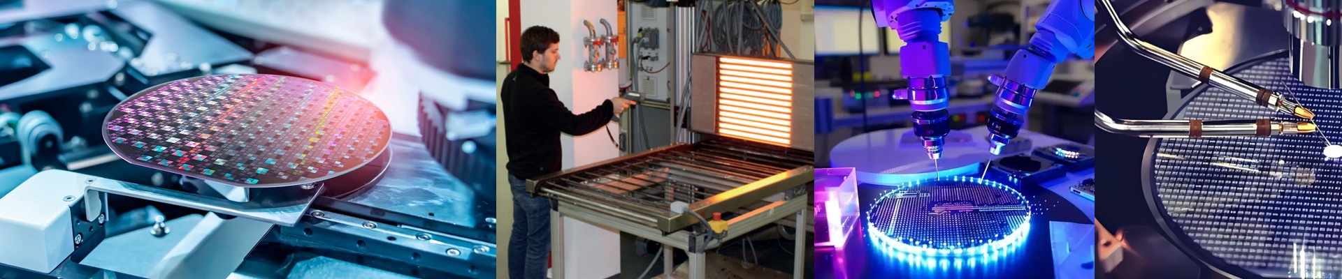
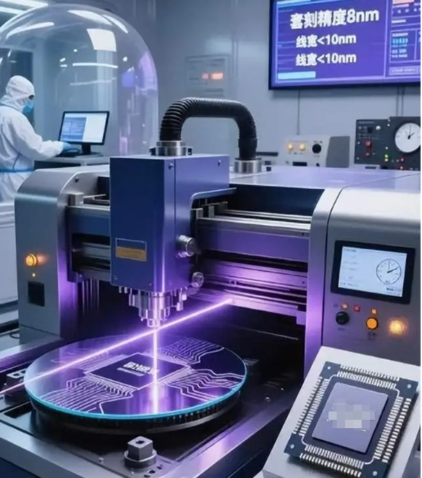
Out on the wafer floor, a half-degree drift in photoresist bake isn’t a “small error.” It’s yield walking out the door. You watch photoresist profiles change, critical dimensions drift, and the line stalls while everyone chases stability. We build semiconductor heaters for the reality of lithography and thermal steps—because in this work, temperature isn’t background noise. It is the process. What matters, technically You need ±0.1°C uniformity across the active zone so every wafer hits the same thermal boundary, wafer to wafer. Cleanroom compatibility isn’t an afterthought—materials, seals, and surface finishes are chosen for Class 1–100 environments, with low outgassing and zero particle generation. The payoff is predictable soft bake and hard bake, consistent photoresist behavior, and thermal budget control you can count on. Why this holds up in a high-volume fab Thermal repeatability keeps excursions down and cuts rework. Tighter uniformity shortens qualification cycles and tightens control limits, which translates to better device performance and more margin. Reliability is engineered for 24/7 operation, so unplanned downtime drops and the scrap tied to thermal issues gets cheaper. You end up with stable output, fewer parameter tweaks, and less energy spent chasing hot and cold spots. The practical details you’ll run into These heaters are compact, so they have to match the chamber geometry and fixturing. Clearance and contact interface directly drive uniformity. Expect fast ramp-up and stable steady-state control, but plan to verify PID tuning and sensor placement during integration. Done right, the unit keeps process stability where it has to be—at the wafer surface.